

Arm’s 2nm Semiconductor Chip Design in Bengaluru: 2025—Why It’s a Game-Changer for India’s Semiconductor Future
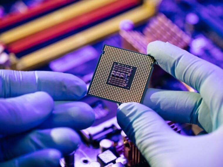
2nm Semiconductor Chip
Welcome to the semiconductor soap opera—full of drama, node names that sound like secret codes (2 nm, 3 nm, not 2 mm!), boardroom twists, and nation-sized ambitions. The latest headline belongs to Arm, the Cambridge-born British 2nm semiconductor chip design powerhouse.
Arm has announced that it will set up an advanced design center in Bengaluru, India, focusing on cutting-edge 2-nanometer (2 nm) chip designs. This isn’t just corporate expansion—it’s a big moment in the global semiconductor race, and it positions India as a serious player in the high-tech world of chips.
What is a 2 nm chip—and why is it revolutionary?
Semiconductors are measured in nanometers (nm)—referring to the size of the transistors carved into silicon wafers. The smaller the number, the more transistors you can pack into the same space, boosting both speed and efficiency.
- 7nm → 5nm → 3nm → 2nm isn’t just marketing jargon.
- 2nm chips bring:
- Up to 45% better energy efficiency
- 25–30% higher performance for AI workloads
- Longer battery life in consumer devices
- Smaller, lighter, and smarter electronics
This makes 2 nm technology the golden ticket for the next generation of smartphones, AI supercomputers, EVs, and even defense tech.
Types and sizes—the semiconductor spectrum
Common node sizes
- 90 nm – 65nm – 45nm: legacy devices, embedded systems
- 28 nm – 14nm: automotive chips, IoT, industrial automation
- 7 nm – 5 nm – 3 nm – 2 nm: cutting-edge for AI accelerators, smartphones, laptops, data centres
For more such interesting articles, please click to our website: https://digiknowledge.co.in/
Chip types and their uses
- Microcontrollers (MCUs): smart appliances, wearables
- System-on-Chip (SoC): smartphones, AR/VR devices
- CPUs & GPUs: laptops, servers, gaming PCs
- AI accelerators (NPUs, TPUs): powering generative AI and machine learning
- Analog & Power ICs: automotive electronics, telecom equipment
- Chiplets & advanced packaging: modular chips that speed up innovation
Where these chips are used
Semiconductor chips are the invisible fuel of the modern world. They are used in:
- Smartphones & Tablets → faster processors, high-resolution cameras, longer battery
- Laptops & PCs → AI-ready CPUs and GPUs
- Cloud & Data Centres → powering ChatGPT-like AI, large-scale analytics
- Automobiles → EV battery management, ADAS, infotainment systems
- 5G Telecom → routers, base stations, RF chips
- Healthcare → wearables, diagnostic machines, AI-enabled scanning tools
- Defence & Space → satellites, secure communication, missile guidance
In short, chips run everything—from the phone in your hand to satellites orbiting above.
The global players—who makes what?
The semiconductor map mirrors world politics:
- Taiwan (TSMC): the leader in 2nm production race
- South Korea (Samsung): advanced nodes and memory leadership
- Japan (Rapidus): working on domestic 2 nm fabs
- United States (Intel, NVIDIA, AMD): design and packaging innovation
- United Kingdom (Arm): IP licensing giant, now stepping into design
- China (SMIC, Huawei): growing but constrained by tech restrictions
Unlike TSMC or Intel, Arm does not manufacture. Instead, it provides blueprints (IP) and earns money through royalties.
The royalty model—how Arm earns
Arm has a unique business model:
- Upfront License Fee: Chipmakers pay to use Arm’s architecture.
- Per-Chip Royalty: every device sold with Arm cores pays a small fee back.
This means:
- Every iPhone, Android, and IoT device contributes royalty revenue to Arm.
- With 2 nm designs, premium royalties will increase.
- By entering into chiplet and AI-specific designs, Arm ensures future-proof income.
It’s a silent gold mine—chips made in Taiwan, Korea, or the US may all still pay royalties to a British company.
Why Arm choosing Bengaluru matters
Bengaluru is often called India’s Silicon Valley, with world-class engineers, start-ups, and labs. Arm’s move signals:
- Trust in Indian talent for high-value chip design
- Knowledge transfer in AI, IoT, and 2nm design
- Job creation in semiconductor R&D
- India’s role shift from consumer to creator in chips
This is not outsourcing—it’s frontline R&D. Bengaluru is joining the league of global chip design capitals.
India’s role now—why this matters
India imports nearly 100% of its chips today. With growing needs in AI, defense, telecom, and EVs, this dependency is dangerous. That’s why the India Semiconductor Mission (ISM) is investing billions to build fabs, OSAT units, and design hubs.
Benefits for India include:
- Boost to GDP and exports
- Creation of tens of thousands of engineering jobs
- Supply chain resilience for defence and critical tech
- Building a domestic innovation ecosystem
India won’t rival TSMC tomorrow, but by focusing on 28–90 nm fabs locally and advanced-node design globally, it can position itself as a serious semiconductor power.
The CEO spotlight—Rene Haas
At the center of Arm’s strategy is Rene Haas, its visionary CEO. Haas has turned Arm into more than just a CPU IP provider. Under his leadership:
- Arm entered AI, cloud, and automotive design
- The company is now eyeing 2nm leadership
- Bengaluru became one of the flagship R&D hubs
For India, this means global visibility, trust in local talent, and direct participation in the semiconductor value chain.
What to watch next
In the next 12–18 months, look out for:
- Test-chip announcements from Bengaluru
- Progress on India’s first fabs (28–90nm nodes)
- Partnerships with TSMC, Samsung, Rapidus for advanced manufacturing
- Hiring booms in Bengaluru’s semiconductor design sector
Final word
The chip war is not about gadgets anymore—it’s about global power, sovereignty, and economic survival.
By placing 2 nm design teams in Bengaluru, Arm has not just expanded its footprint—it has pushed India into the center of the world’s semiconductor conversation.
India may not build a TSMC overnight. But with fab capacity at mature nodes and design leadership at advanced nodes, it is laying the foundation for true semiconductor independence.
Bengaluru isn’t just coding the future anymore. It’s designing the future of chips.
Disclaimer:
The information presented in this article is compiled from various news updates, industry insights, and technology reports. While every effort has been made to ensure accuracy, some details may change over time as the semiconductor industry evolves.
Readers are advised to verify specific technical or investment-related information with official sources or professional guidance.
This article is intended purely for informational and educational purposes and should not be taken as financial, technical, or business advice.


